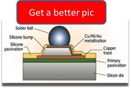
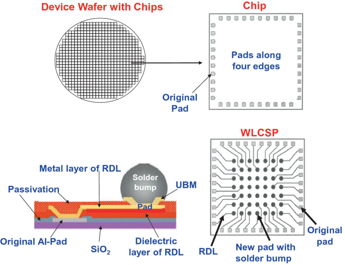
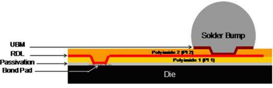
The bond pad redistribution layer (polyimide 1) and the under bump

Process integration of fine pitch Cu redistribution wiring and SnCu micro-bumping for power efficient LSI devices with high-bandwidth stacked DRAM - ScienceDirect

Yes RDL Explanation, PDF, Building Engineering
Polymers in Electronics Part Six: Redistribution Layers for Fan-Out Wafer Level Packaging - Polymer Innovation Blog

Warren FLACK, Vice President, PhD

Repassivation Design Guide
Materials, Free Full-Text
Fan-In Wafer/Panel-Level Chip-Scale Packages

Process and Key Technology of Typical Advanced Packaging

Polymers, Free Full-Text

Electromigration Performance Of Fine-Line Cu Redistribution Layer (RDL) For HDFO Packaging

A review on numerical approach of reflow soldering process for copper pillar technology

PDF) Characterization study of an aqueous developable photosensitive polyimide on 300-mm wafers
Redistribution Layer (RDL) Technology for ICs Package

The bond pad redistribution layer (polyimide 1) and the under bump
Chip Scale Packaging Helps Portable Medical Devices Save Size and Weight