Wire Bonding, a Way to Stitch Chips to PCBs - SK hynix Newsroom
To each sheet of wafers that have completed the front-end process, 500 to 1,200 chips, which can be also called dies, are attached.
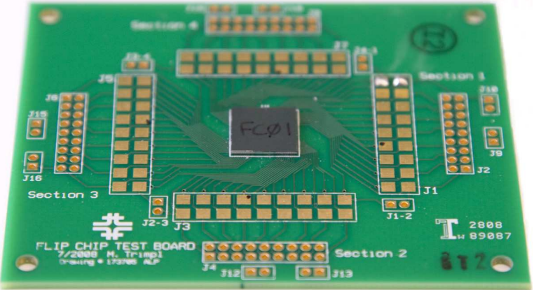
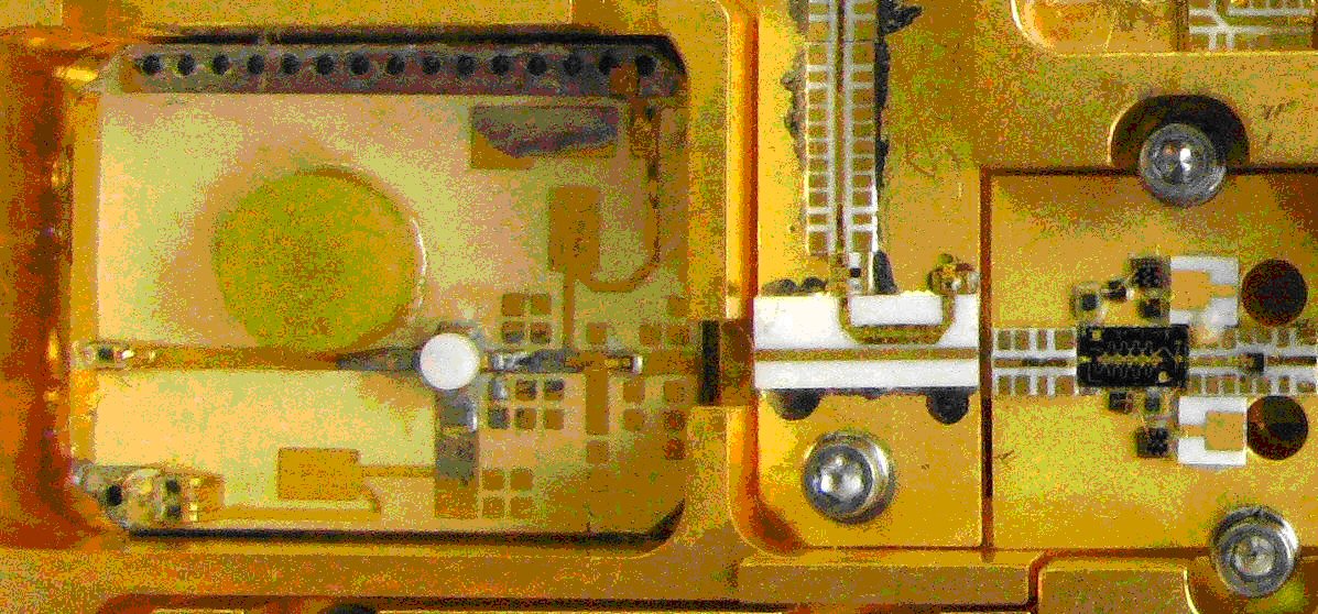
PCB Design Rules for Chip-on-Board Layout

Jong-moon Jin - SK hynix Newsroom
_%EC%88%98%EC%A0%95.jpg?type=w800&jopt=2)
반도체 후공정 - SK hynix : 네이버 블로그
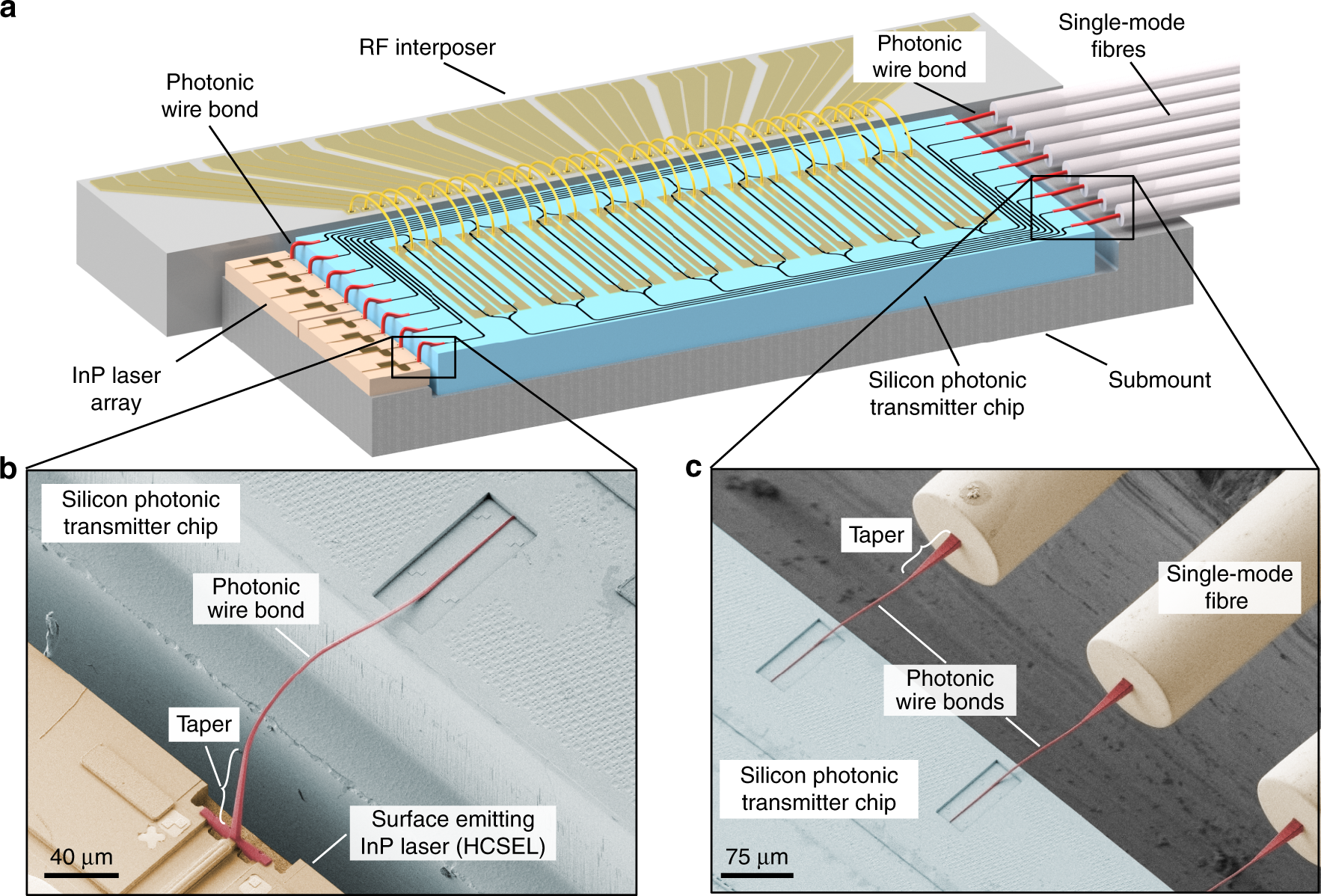
Hybrid multi-chip assembly of optical communication engines by in situ 3D nano-lithography
d36ae2cxtn9mcr.cloudfront.net/wp-content/uploads/2

PCB Design Rules for Chip-on-Board Layout
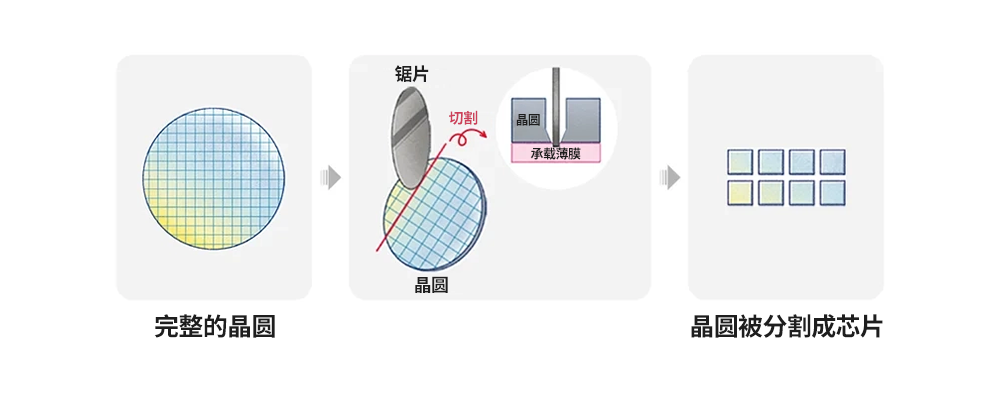
传统封装方法组装工艺的八个步骤(上)-电子发烧友网

PDF) Progress and challenges of EUV lithography for high-volume manufacturing (Invited Paper)

d36ae2cxtn9mcr.cloudfront.net/wp-content/uploads/2
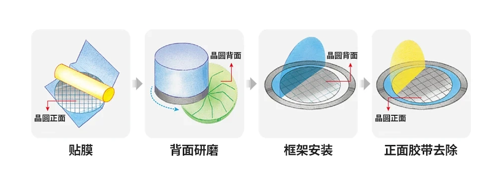
传统封装方法组装工艺的八个步骤(上)-电子发烧友网

Wire Bonding, a Way to Stitch Chips to PCBs - SK hynix Newsroom

d36ae2cxtn9mcr.cloudfront.net/wp-content/uploads/2
Microwaves101 Chip & Wire Construction

반도체 후공정 - SK hynix : 네이버 블로그